Quantum Dot Architecture Nanodynamics:
Self-assembled semiconductor quantum dots (QDs) are the subject of world-wide interest because of their potential use in quantum information technologies and nanoscale optoelectronics. The goal is to create advanced QD architectures by controlling the precise position of single dots or molecules during epitaxial growth. However, a significant limitation in the realisation of site controlled III-V quantum structures is our inability to observe how they form in real-time and hence understand how to precisely tailor their characteristics. This project will utilise a unique electron microscope in Cardiff to obtain the first real-time movies of how QDs actually form in advanced architectures. By addressing the key issues of precise site control and narrow optical line-width it will, for example, facilitate the large scale integration of QDs into quantum photonic circuits and networks for uses in quantum computation
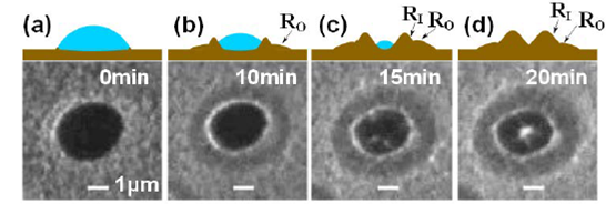
Figure from: Y. Zhou, C. X. Zheng, W. X. Tang, J. Tersoff and D. E. Jesson, Phys. Rev. Lett. 111, (2013) 036102.
Tersoff, D. E. Jesson and W. X. Tang, Science 324, (2009) 236.
Tersoff, D. E. Jesson and W. X. Tang, Phys. Rev. Lett. 105, (2010) 035702.
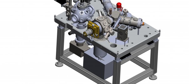
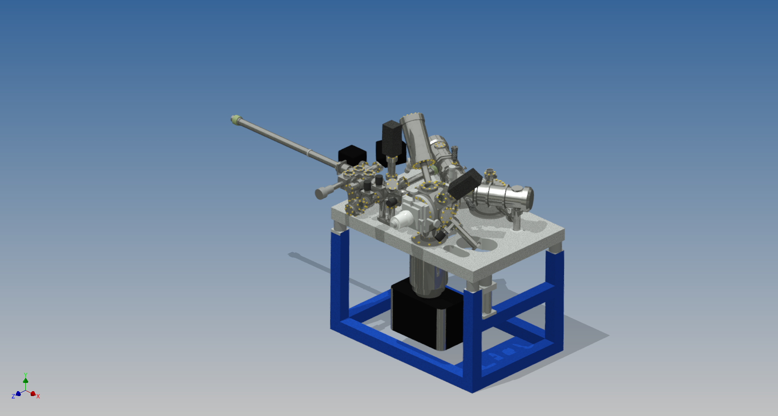
Instrumentation project Development of state-of-the-art Molecular Beam Epitaxy – Low Energy Electron Microscope (MBE-LEEM) to study epitaxial dynamics
An MBE-LEEM system will be developed, combining in-situ state-of-the-art Molecular Beam Epitaxy and a Low Energy Electron Microscope. The project will increase capabilities in sample exchange, increase reproducibility and accuracy of flux measurements, increase reproducibility and accuracy of temperature control, increase the number of material sources, enabling the growth of new materials, increase safety, reduce down-time of the system and increase control during surface preparation.
Nanostructure nucleation dynamics (USEMITE-MSCA)
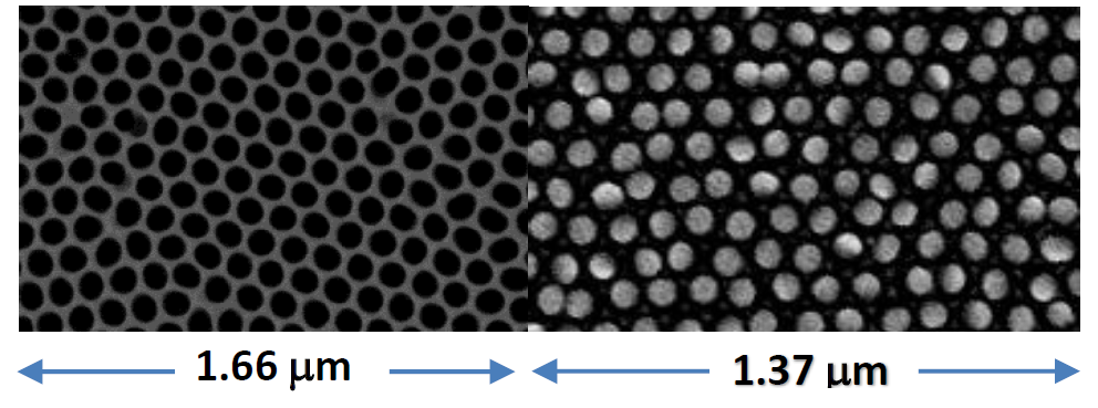
The project will combine the study of growth dynamics and defect dynamics during epitaxy of GaAs thin films, quantum wires and quantum dots. Anodized Aluminium Oxide (AAO) membranes will be used to generate nucleation points for nanowires across large areas of the samples. Catalyst assisted nucleation, self-assisted nucleation and selective area growth will be imaged in real time using our state-of-the-art MBE-LEEM system. Nucleation of QDs grown using Stransky-Krastanov growth mode, droplet epitaxy and QW epitaxy will be compared. Complex templates grown in state-of-the-art MBE facilities will be used as substrates to study nucleation dynamics as a function of strain field.