Molecular Beam Epitaxy is the name of the technique we use to grow extremely thin crystalline layers. Within a Molecular Beam Epitaxy chamber a very low number of molecules or atoms can be found. It is carried out in what is called Ultra High Vacuum (UHV) – 10-9 to 10-13 Torr.
Our starting point is a substrate, a crystal that is as similar as possible to the crystal we want to grow, and that will serve, in some sense, as a mold or cast for the new crystal to grow.
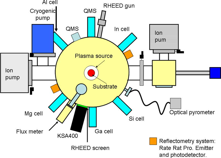
We send beams of atoms or molecules onto our substrate. These atoms or molecules originate from the sublimation of the material in small furnaces called Knudsen cells or effusion cells. Because there are barely any atoms or molecules floating in the system, the sublimated atoms behave as a precise beam. By calculating the number of atoms/molecules that arrive to the substrate, we can set the ratio between the number of atoms of different elements that reach the substrate at a certain time.
Different materials require different ratios, as an example, if we were to grow Gallium Nitride, we would adjust our beams so we have the same amount of Ga and Nitrogen arriving to the substrate. and if we are to grow Strontium Titanate (SrTiO3), we would adjust our beams to have 1 part of Strontium, 1 part of Ti and 3 parts of oxygen. Of course, it is usually more complicated than this, depending on the temperature the substrate is at, and the materials you are growing, there are a number of processes you have to take into account, atom mobility on the surface, desorption, incorporation, etc.
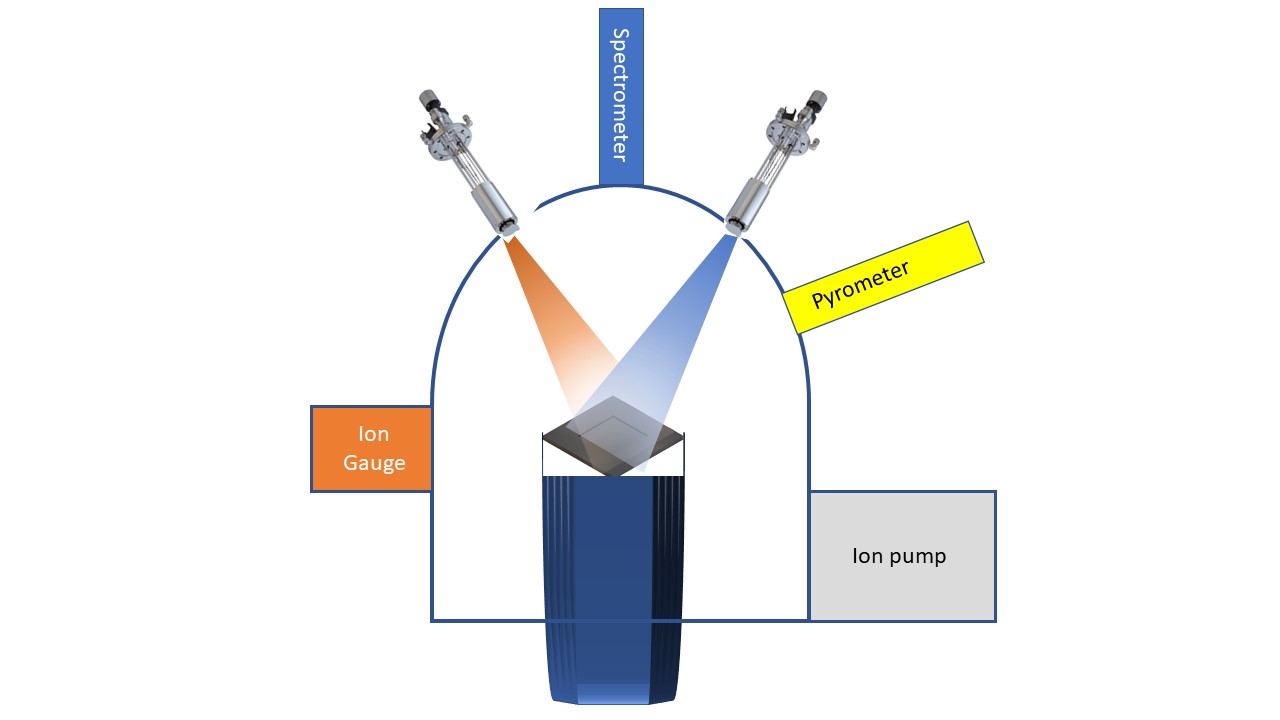
There are a number of ways to monitor the growth of thin crystalline layers. Reflection High Energy Electron Diffraction (RHEED) consists of an electron gun that sends electrons that graze the surface of the sample. Since they just graze the sample, they are very sensitive to its surface, and the diffraction patterns of this electrons allow us to know about the crystal structure of the surface. Mass Spectrometry, Laser interferometry and many other more sophisticated techniques are used to monitor the growth rate of samples or the atom desorption from it.
Molecular Beam Epitaxy was developed around 1968 at Bell Laboratories by two American physicists, Chinese-born Alfred Y. Cho and John R. Arthur, Jr. Important contributions were also made by other scientists, such as Japanese-born physicist Leo Esaki (who won the 1973 Nobel Prize in Physics for his work on semiconductor electronics) and Ray Tsu, working at IBM.