Low-energy electron microscopy, or LEEM, was invented by Ernst Bauer in 1962, however, not fully developed (by Ernst Bauer and Wolfgang Telieps) until 1985.
LEEM is a technique used by to image crystalline surfaces and processes that happen on those surfaces, for example atom-surface interactions, growth of thin crystalline films, movement of atomic steps in a crystal, defects in a crystal, etc.
In LEEM, an electron gun emits a beam of high energy electrons. The electrons are focused using a set of electromagnetic lenses, and sent through a magnetic beam splitter, which bends the beam towards an electromagnetic objective lens.
A large voltage difference is set between the objective and the sample, what decelerate the electrons to low energies (0-100 eV). The low-energy electrons are “surface-sensitive”, meaning they will arrive so slow to the sample that they will just interact with its surface. The near-surface sampling depth can be varied by tuning the energy of the incident electrons. When the electrons interact with the sample they “bounce back”, travel back through the objective lens, reaccelerate, and pass through the beam splitter again. However, now the electrons travel in the opposite direction and the beam splitter sends them opposite to the electron gun, and towards the detector.
Different imaging conditions allow to either look at the diffraction pattern (low-energy electron diffraction, LEED) of the surface, or at the actual real image of the surface in real time. Therefore allowing to make movies of the process we are imaging, for example, videos of the formation of the crystals, or videos of atomic layers moving, or very small islands of material forming.
The phenomena that can be observed include (but are not limited to): tomography, phase transitions, adsorption, reaction, segregation, thin film growth, etching, strain relief, sublimation, and magnetic microstructure.
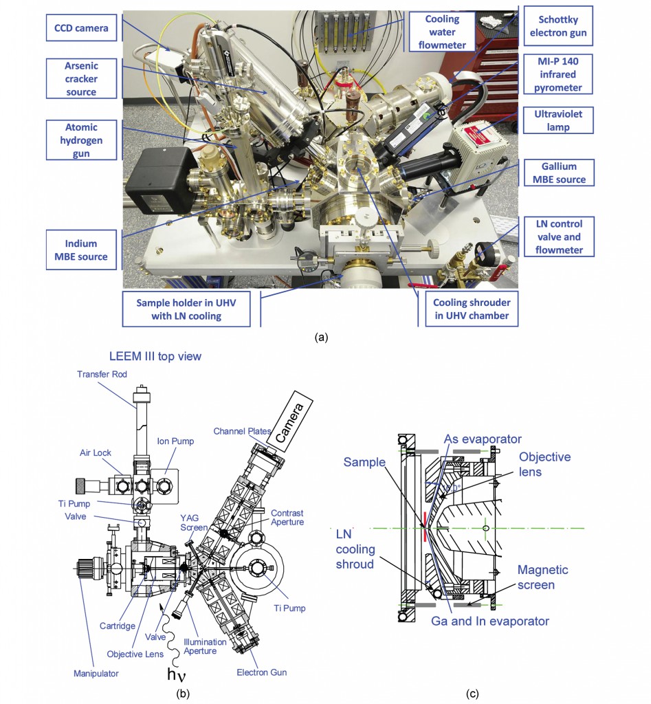
Our system consists of a Low Energy Electron Microscope (LEEM) and an MBE system with 2 knudsen cells, an As cracker and a Hydrogen ion gun. The LEEM enables real space imaging of the surface with a resolution around 5 nm in the x-y plane, and atomic resolution in the z-axis (which is obtained by tuning the energy of the impinging electrons). By changing the electron optics configuration, it is possible to switch from LEEM to micro-spot Low Energy Electron Diffraction (um-LEED). Illuminating the surface with an UV light source, one can also measure Photo-emission electron microscopy (PEEM). By filtering a particular diffraction spot in the back focal plane of the objective lens, phase sensitivity can be achieved, i.e. contrast between phases with different atomic structures will be observed in the real-space image.
The instrument is highly versatile, and able to provide information that cannot be obtained through any other technique, since it provides information on the dynamics of the growth.